Journals > > Topics > Thin Films
Thin Films|87 Article(s)
Investigation of Stress Fields in the in situ Manufacturing of Composite Alumina Ceramic Coatings by Laser Cladding
Yuyan Zhang, Wei Fang, Chen Li, and Yintang Wen
Considering the significant influence of thermal stress on the coating quality during the in situ fabrication of new iron particle-reinforced alumina coating by laser melting, we investigated the thermal stress of a single-pass composite alumina coating on the surface of titanium alloy in this study. The representative volume element method was used to simulate and calculate the thermodynamic parameters of the new coating. The heat source model of the laser-induced thermal reaction heat was established using a combination of the raw-dead cell method and internal raw-dead heat source. The thermal stress distribution pattern of the coating components at the end of the cladding under different combinations of process parameters was calculated and analyzed. The results indicate that the thermal stresses are primarily concentrated in the coating and its bonding surface with the substrate and the tensile stresses on the coating along the melting direction are the main causes of transverse cracks in the coating. Owing to the laser-induced thermal reaction, the coating cracks increase with laser power and laser scanning speed. At 600 W laser power, the coating has the lowest number of cracks when the scanning speed is 2 mm/s. Moreover, at a scanning speed of 5 mm/s, the coating has the lowest residual stresses when the laser power is 300 W. Considering the significant influence of thermal stress on the coating quality during the in situ fabrication of new iron particle-reinforced alumina coating by laser melting, we investigated the thermal stress of a single-pass composite alumina coating on the surface of titanium alloy in this study. The representative volume element method was used to simulate and calculate the thermodynamic parameters of the new coating. The heat source model of the laser-induced thermal reaction heat was established using a combination of the raw-dead cell method and internal raw-dead heat source. The thermal stress distribution pattern of the coating components at the end of the cladding under different combinations of process parameters was calculated and analyzed. The results indicate that the thermal stresses are primarily concentrated in the coating and its bonding surface with the substrate and the tensile stresses on the coating along the melting direction are the main causes of transverse cracks in the coating. Owing to the laser-induced thermal reaction, the coating cracks increase with laser power and laser scanning speed. At 600 W laser power, the coating has the lowest number of cracks when the scanning speed is 2 mm/s. Moreover, at a scanning speed of 5 mm/s, the coating has the lowest residual stresses when the laser power is 300 W.
Laser & Optoelectronics Progress
- Publication Date: May. 10, 2023
- Vol. 60, Issue 9, 0931001 (2023)

Magnetron Sputtering Preparation and Photoelectric Property Optimization of GAZO/Ag/GAZO Transparent Conductive Thin Films
Junchen Liao, Rui Qian, Dong Chen, Haijin Chen, Guoping Luo, and Weiling Zhu
Multisource magnetron sputtering technology was used to prepare Ga and Al co-doped zinc oxide (GAZO)/Ag/GAZO transparent conductive thin films on a glass substrate. Comparative experiments showed that sputtering Ag with oxygen can increase the optical transmittance of the thin films in the 600-800 nm spectral region. After further optimization, at an oxygen flow of 1.0 sccm, Ag films with a thickness of 12 nm obtained continuous structure, which improved the photoelectric properties of the GAZO/Ag/GAZO thin films. Subsequent annealing at 150 ℃ for 1 h under ambient pressure further improved the photoelectric and structural properties of GAZO/Ag/GAZO thin films. After annealing, the sheet resistance of the thin films is 8.99 Ω/sq, the average transmittance in the 380-780 nm visible region is 98.17%, and the figure of merit is as high as 2260 Ω-1. The prepared GAZO/Ag/GAZO transparent conductive thin films show excellent photoelectric properties and are expected to replace indium tin oxide films in the field of optoelectronic devices. Multisource magnetron sputtering technology was used to prepare Ga and Al co-doped zinc oxide (GAZO)/Ag/GAZO transparent conductive thin films on a glass substrate. Comparative experiments showed that sputtering Ag with oxygen can increase the optical transmittance of the thin films in the 600-800 nm spectral region. After further optimization, at an oxygen flow of 1.0 sccm, Ag films with a thickness of 12 nm obtained continuous structure, which improved the photoelectric properties of the GAZO/Ag/GAZO thin films. Subsequent annealing at 150 ℃ for 1 h under ambient pressure further improved the photoelectric and structural properties of GAZO/Ag/GAZO thin films. After annealing, the sheet resistance of the thin films is 8.99 Ω/sq, the average transmittance in the 380-780 nm visible region is 98.17%, and the figure of merit is as high as 2260 Ω-1. The prepared GAZO/Ag/GAZO transparent conductive thin films show excellent photoelectric properties and are expected to replace indium tin oxide films in the field of optoelectronic devices.
Laser & Optoelectronics Progress
- Publication Date: Apr. 10, 2023
- Vol. 60, Issue 7, 0731002 (2023)
Preparation and Sensing Properties of Pt-WO3 Nano-Hydrogen-Sensitive Film
Xingquan Wang, and Zhenglan Bian
The tungsten trioxide sol is prepared using the tungsten powder-hydrogen peroxide-polytungstic acid method, doped using chloroplatinic acid, and spin-coated into a platinum-doped nanotungsten trioxide film exhibiting hydrogen-induced discoloration. The film properties are analyzed using X-ray diffraction, field-emission scanning electron microscopy, and energy-dispersive spectroscopy. The film is amorphous and exhibits a flat, bump- and crack-free surface over which platinum metal and loose porous-structured tungsten trioxide particles are evenly distributed. A transmission optical-fiber hydrogen sensor system is fabricated using the prepared film. When hydrogen molecules are present, the film chemically reacts through platinum catalysis, thereby changing the film refractive index. The hydrogen concentration is determined by measuring the transmitted light intensity. The hydrogen-sensitive film spin-coated for 60 s using a homogenizer rotating at 3100 r/min and subsequently annealed at 400 ℃ for 60 min exhibits a hydrogen-passing response time of approximately 62 s at a H2 concentration of 5%. The average change rate of the signal response amplitude is 91.54% before and after hydrogen sensing, and the film exhibits good repeatability and stability. The tungsten trioxide sol is prepared using the tungsten powder-hydrogen peroxide-polytungstic acid method, doped using chloroplatinic acid, and spin-coated into a platinum-doped nanotungsten trioxide film exhibiting hydrogen-induced discoloration. The film properties are analyzed using X-ray diffraction, field-emission scanning electron microscopy, and energy-dispersive spectroscopy. The film is amorphous and exhibits a flat, bump- and crack-free surface over which platinum metal and loose porous-structured tungsten trioxide particles are evenly distributed. A transmission optical-fiber hydrogen sensor system is fabricated using the prepared film. When hydrogen molecules are present, the film chemically reacts through platinum catalysis, thereby changing the film refractive index. The hydrogen concentration is determined by measuring the transmitted light intensity. The hydrogen-sensitive film spin-coated for 60 s using a homogenizer rotating at 3100 r/min and subsequently annealed at 400 ℃ for 60 min exhibits a hydrogen-passing response time of approximately 62 s at a H2 concentration of 5%. The average change rate of the signal response amplitude is 91.54% before and after hydrogen sensing, and the film exhibits good repeatability and stability.
Laser & Optoelectronics Progress
- Publication Date: Apr. 10, 2023
- Vol. 60, Issue 7, 0731001 (2023)
Development of Longwave Infrared Antireflective Coating Based on As40Se60 Chalcogenide Glass
Zhuo Liu, Youliang Zhang, Gang Li, Weisheng Yang, Xueying Wang, Qiming Xie, and Xiaojing Yang
Infrared optical coatings deposited on the As40Se60 chalcogenide glass have the disadvantage of poor adhesion. The firmness of the coating has been a major research object to solve the problem of coating adhesion. First, the appropriate film source materials were chosen, and the design and optimization of the film system were completed. The single factor experiment was carried out with the deposition temperature as the influencing factor, and the deposition process and residual stress of the ZnS connection layer were examined. The method without an ion source was used to reduce the residual stress of the connection layer and improve film adhesion. Finally, the problem of coating adhesion at higher temperatures was solved. An infrared antireflective coating with an 8-12 μm wavelength was developed, and the deposition process was applied to practical production. The average transmittance and reflectance of the prepared film were 98% and 0.6%, respectively. The adhesion, high and low temperature, and humidity experiment met the requirements of the GJB2845—1995 standard. Infrared optical coatings deposited on the As40Se60 chalcogenide glass have the disadvantage of poor adhesion. The firmness of the coating has been a major research object to solve the problem of coating adhesion. First, the appropriate film source materials were chosen, and the design and optimization of the film system were completed. The single factor experiment was carried out with the deposition temperature as the influencing factor, and the deposition process and residual stress of the ZnS connection layer were examined. The method without an ion source was used to reduce the residual stress of the connection layer and improve film adhesion. Finally, the problem of coating adhesion at higher temperatures was solved. An infrared antireflective coating with an 8-12 μm wavelength was developed, and the deposition process was applied to practical production. The average transmittance and reflectance of the prepared film were 98% and 0.6%, respectively. The adhesion, high and low temperature, and humidity experiment met the requirements of the GJB2845—1995 standard.
Laser & Optoelectronics Progress
- Publication Date: Mar. 10, 2023
- Vol. 60, Issue 5, 0531003 (2023)
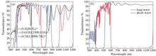
Study on Band Pass Filter with Wide Cutoff and High Q Factor
Jinglong Yan, Yixiang Wang, Huaxin Zhu, Dongsheng Rao, and Tao Liu
TiO2 and SiO2 are selected as high and low refractive index materials, and the sapphire substrate wide cutoff high Q factor band pass filter is designed by traditional design method (the long wave and short wave pass film systems are plated on both sides of the substrate, with the thickness of 1.67 μm and 8.67 μm, respectively). In order to avoid the problem of large variation of filter one-sided shape caused by large difference of film thickness, the membrane system on both sides of the substrate is rearranged. After optimization, the number of film layers on both sides is 49 and 50, and the thickness of film layer is 5.73 μm and 4.22 μm, respectively. The thin films are plated by electron beam evaporation physical vapor deposition and the transmittance of the samples is measured by spectrophotometer. The experimental results show that the average transmittance of the sample in the passband (521-596 nm) is 96.59%, the average transmittance in the cutoff region is 0.076%, the rectangularity of the passband is 0.95, and the steepness of the transition zone on both sides of the passband is 0.89%. It has the characteristics of high Q factor filter. In addition, the experimental curve is in good agreement with the design curve, which verifies the effectiveness of optimizing the structure of the two-sided membrane system. TiO2 and SiO2 are selected as high and low refractive index materials, and the sapphire substrate wide cutoff high Q factor band pass filter is designed by traditional design method (the long wave and short wave pass film systems are plated on both sides of the substrate, with the thickness of 1.67 μm and 8.67 μm, respectively). In order to avoid the problem of large variation of filter one-sided shape caused by large difference of film thickness, the membrane system on both sides of the substrate is rearranged. After optimization, the number of film layers on both sides is 49 and 50, and the thickness of film layer is 5.73 μm and 4.22 μm, respectively. The thin films are plated by electron beam evaporation physical vapor deposition and the transmittance of the samples is measured by spectrophotometer. The experimental results show that the average transmittance of the sample in the passband (521-596 nm) is 96.59%, the average transmittance in the cutoff region is 0.076%, the rectangularity of the passband is 0.95, and the steepness of the transition zone on both sides of the passband is 0.89%. It has the characteristics of high Q factor filter. In addition, the experimental curve is in good agreement with the design curve, which verifies the effectiveness of optimizing the structure of the two-sided membrane system.
Laser & Optoelectronics Progress
- Publication Date: Mar. 10, 2023
- Vol. 60, Issue 5, 0531002 (2023)

Ultraviolet Narrow Band Antireflection of Fe Nanoparticles Embedded in MgO Films
Jinjing Fang, Linhong Cao, Jian Yu, Jin Wang, Yajun Fu, Wanting Lan, Jingsong Zhang, and Weidong Wu
Fe/MgO nanocomposite films are prepared using pulsed laser deposition, and the effects of pulse number on the structure, composition, and optical properties of the composite films are studied in this paper. X-ray diffraction analysis shows that a diffraction peak with a crystal plane orientation of (211) appears when the pulse number of the deposited Fe nanoparticles is greater than 500, confirming the existence of Fe, Mg, and O elements in the composite film; part of the Fe nanoparticles in MgO film is oxidized, thus existing in the elemental and oxidized states (content ratio of ~3∶2). High-resolution transmission electron microscopy analysis shows that when the pulse number is 100, Fe nanoparticles with an average particle size of ~2.73 nm are uniformly distributed in an ellipsoid shape in the MgO film, and the average spacing between Fe nanoparticles is ~1.75 nm. Ellipsometry analysis shows that the refractive index and dispersion sensitivity of the Fe/MgO nanocomposite films increases as the pulse number increasing when the wavelength is less than 365 nm. Ultraviolet-visible spectral analysis shows that Fe/MgO nanocomposite films exhibit an obvious ultraviolet narrow-band antireflection phenomenon in the wavelength range of 190-235 nm compared with pure MgO films;the transmittance of the composite film at 197 nm is ~69.4%. Fe/MgO nanocomposite films are prepared using pulsed laser deposition, and the effects of pulse number on the structure, composition, and optical properties of the composite films are studied in this paper. X-ray diffraction analysis shows that a diffraction peak with a crystal plane orientation of (211) appears when the pulse number of the deposited Fe nanoparticles is greater than 500, confirming the existence of Fe, Mg, and O elements in the composite film; part of the Fe nanoparticles in MgO film is oxidized, thus existing in the elemental and oxidized states (content ratio of ~3∶2). High-resolution transmission electron microscopy analysis shows that when the pulse number is 100, Fe nanoparticles with an average particle size of ~2.73 nm are uniformly distributed in an ellipsoid shape in the MgO film, and the average spacing between Fe nanoparticles is ~1.75 nm. Ellipsometry analysis shows that the refractive index and dispersion sensitivity of the Fe/MgO nanocomposite films increases as the pulse number increasing when the wavelength is less than 365 nm. Ultraviolet-visible spectral analysis shows that Fe/MgO nanocomposite films exhibit an obvious ultraviolet narrow-band antireflection phenomenon in the wavelength range of 190-235 nm compared with pure MgO films;the transmittance of the composite film at 197 nm is ~69.4%.
Laser & Optoelectronics Progress
- Publication Date: Mar. 10, 2023
- Vol. 60, Issue 5, 0531001 (2023)
Optimization Analysis of Dual-Interface Grating Structures for Thin Film Solar Cells
Ke Chen, Sheng Wu, Hongmei Zheng, Wenli Tian, and Zhijie Liu
A structure of the front semicircle and rear trapezoidal dual-interface grating monocrystalline silicon thin film solar cell was designed. The structure and the control group were simulated by the finite-difference time-domain method. It is shown that the dual-interface has better light-trapping performance than the single-interface grating structure by analysis of the short circuit current density and absorption spectrum. The absorption enhancement mechanism of the structure at long wavelength (750-1100 nm) was analyzed by using electromagnetic field distribution. In addition, for the front semicircle rear trapezoidal grating structure, the left and right slope of rear trapezoidal grating and the offset degree of front and rear gratings under the same period are further optimized. The results show that the irregular trapezoidal gratings have better light-trapping performance, and through the absorption efficiency cloud diagram, the best effect can be found when the offset degree is at 40 nm. The optimal short-circuit current density reaches 20.17 mA/cm2, which is 58.1% higher than the planar structure by calculation and analysis. The research results have certain guiding significance for the grating structure design of thin film solar cells. A structure of the front semicircle and rear trapezoidal dual-interface grating monocrystalline silicon thin film solar cell was designed. The structure and the control group were simulated by the finite-difference time-domain method. It is shown that the dual-interface has better light-trapping performance than the single-interface grating structure by analysis of the short circuit current density and absorption spectrum. The absorption enhancement mechanism of the structure at long wavelength (750-1100 nm) was analyzed by using electromagnetic field distribution. In addition, for the front semicircle rear trapezoidal grating structure, the left and right slope of rear trapezoidal grating and the offset degree of front and rear gratings under the same period are further optimized. The results show that the irregular trapezoidal gratings have better light-trapping performance, and through the absorption efficiency cloud diagram, the best effect can be found when the offset degree is at 40 nm. The optimal short-circuit current density reaches 20.17 mA/cm2, which is 58.1% higher than the planar structure by calculation and analysis. The research results have certain guiding significance for the grating structure design of thin film solar cells.
Laser & Optoelectronics Progress
- Publication Date: Apr. 10, 2022
- Vol. 59, Issue 7, 0731001 (2022)
Effect of Energy Density on Structure and Properties of a Laser Cladding Molybdenum Layer
Shengyuan Lei, Zhimin Cai, Xincheng Jiang, Haili Huang, Yifei Dai, and Weizhou Li
A molybdenum cladding layer was prepared by laser cladding technology with a preset powder to improve the comprehensive properties of Nb alloy. The microstructure, crack rate, hardness, and wear resistance of the laser cladding layer with different energy densities were analyzed using a metallographic microscope, scanning electron microscope, X-ray diffraction, microhardness tester, and friction and wear tester. The findings show that when the energy density was 6.67 J/mm2, the surface of the cladding layer was smooth and the weld path was regular and continuous. The hardness of the cladding layer increased from 420 HV0.05 to 480 HV0.05 when the energy density was increased from 5.56 J/mm2 to 8.90 J/mm2, while the wear rate decreased from 12.24×10⁻³ mg/m to 7.59×10⁻³ mg/m, showing a 38% decrease. The phase of the cladding layer was mainly a Nb-Mo solid solution, with a Mo content of up to 22.3%. After 5 h of corrosion with 10% HF acid, no grain boundaries of the cladding layer were found, and the corrosion resistance of the cladding layer to HF acid showed significant improvement. In conclusion, the comprehensive performance of the niobium alloy can be improved by preparing a molybdenum cladding layer by laser cladding. A molybdenum cladding layer was prepared by laser cladding technology with a preset powder to improve the comprehensive properties of Nb alloy. The microstructure, crack rate, hardness, and wear resistance of the laser cladding layer with different energy densities were analyzed using a metallographic microscope, scanning electron microscope, X-ray diffraction, microhardness tester, and friction and wear tester. The findings show that when the energy density was 6.67 J/mm2, the surface of the cladding layer was smooth and the weld path was regular and continuous. The hardness of the cladding layer increased from 420 HV0.05 to 480 HV0.05 when the energy density was increased from 5.56 J/mm2 to 8.90 J/mm2, while the wear rate decreased from 12.24×10⁻³ mg/m to 7.59×10⁻³ mg/m, showing a 38% decrease. The phase of the cladding layer was mainly a Nb-Mo solid solution, with a Mo content of up to 22.3%. After 5 h of corrosion with 10% HF acid, no grain boundaries of the cladding layer were found, and the corrosion resistance of the cladding layer to HF acid showed significant improvement. In conclusion, the comprehensive performance of the niobium alloy can be improved by preparing a molybdenum cladding layer by laser cladding.
Laser & Optoelectronics Progress
- Publication Date: Mar. 10, 2022
- Vol. 59, Issue 5, 0531001 (2022)
Design and Simulation of Nonlocal Perfect Absorption Thin Film
Jianxiao Liu, Li Zhang, Jingjing Du, Xiaolan Liu, and Linghui Meng
Finite-difference time-domain (FDTD) methods often require smaller spatial discrete steps when calculating the nonlocal properties of metal nanostructures, which brings difficulties to the calculation when the model size is large. However, due to the introduction of longitudinal wave vector, the hydrodynamic model describing the properties of the metal nonlocal property is inconvenient for the calculation of semi-analytical methods such as the transfer matrix method (TMM). Therefore, a method combining FDTD and TMM to solve the absorptivity of nano-metal nonlocal thin films is proposed in this paper. The reflection coefficient and transmission coefficient of the metal are obtained by the FDTD method, and the equivalent dielectric constant of the nonlocal metal is obtained by inversion. Substitute the equivalent permittivity and model parameters into the TMM, and the electromagnetic properties of the complete structure are calculated. The results show that this method can solve the problem of insufficient memory caused by small grid of FDTD and the computational complexity caused by longitudinal wave vector in TMM, and calculations of reflectivity, transmittance, and absorptivity of layered nanostructures can be performed quickly. Finite-difference time-domain (FDTD) methods often require smaller spatial discrete steps when calculating the nonlocal properties of metal nanostructures, which brings difficulties to the calculation when the model size is large. However, due to the introduction of longitudinal wave vector, the hydrodynamic model describing the properties of the metal nonlocal property is inconvenient for the calculation of semi-analytical methods such as the transfer matrix method (TMM). Therefore, a method combining FDTD and TMM to solve the absorptivity of nano-metal nonlocal thin films is proposed in this paper. The reflection coefficient and transmission coefficient of the metal are obtained by the FDTD method, and the equivalent dielectric constant of the nonlocal metal is obtained by inversion. Substitute the equivalent permittivity and model parameters into the TMM, and the electromagnetic properties of the complete structure are calculated. The results show that this method can solve the problem of insufficient memory caused by small grid of FDTD and the computational complexity caused by longitudinal wave vector in TMM, and calculations of reflectivity, transmittance, and absorptivity of layered nanostructures can be performed quickly.
Laser & Optoelectronics Progress
- Publication Date: Nov. 10, 2022
- Vol. 59, Issue 21, 2131001 (2022)
High Crystallization Quality β-Ga2O3 Films Prepared by Chemical Vapor Deposition
Xingchen Li, Fengyuan Lin, Huimin Jia, Yubin Kang, Yongji Shi, Bingheng Meng, Dan Fang, Jilong Tang, Dengkui Wang, Kexue Li, Xueying Chu, and Zhipeng Wei
In order to obtain high-quality films and reduce experimental costs, β-Ga2O3 films were synthesized on mica substrates by chemical vapor deposition using GaTe powder as the Ga source. High crystalline quality β-Ga2O3 thin films were obtained by changing the growth temperature, buffer gas, and growth time, which were confirmed by X-ray diffraction (XRD) and Raman spectroscopy. XRD results showed that the optimal growth temperature of the film was 750 ℃. A comparison of β-Ga2O3 films synthesized under different buffer gases revealed Ar to be the best environment for growing film materials. The growth time of the thin films was changed under an Ar atmosphere to achieve β-Ga2O3 thin films with high crystalline quality. XRD results showed that the thin film with a growth time of 20 min had high crystalline quality. Finally, it was transferred to a Si/SiO2 substrate with a 300 nm thick oxide layer and tested by atomic force microscopy to obtain a 16 nm thick two-dimensional Ga2O3 film. In order to obtain high-quality films and reduce experimental costs, β-Ga2O3 films were synthesized on mica substrates by chemical vapor deposition using GaTe powder as the Ga source. High crystalline quality β-Ga2O3 thin films were obtained by changing the growth temperature, buffer gas, and growth time, which were confirmed by X-ray diffraction (XRD) and Raman spectroscopy. XRD results showed that the optimal growth temperature of the film was 750 ℃. A comparison of β-Ga2O3 films synthesized under different buffer gases revealed Ar to be the best environment for growing film materials. The growth time of the thin films was changed under an Ar atmosphere to achieve β-Ga2O3 thin films with high crystalline quality. XRD results showed that the thin film with a growth time of 20 min had high crystalline quality. Finally, it was transferred to a Si/SiO2 substrate with a 300 nm thick oxide layer and tested by atomic force microscopy to obtain a 16 nm thick two-dimensional Ga2O3 film.
Laser & Optoelectronics Progress
- Publication Date: Oct. 10, 2022
- Vol. 59, Issue 19, 1931003 (2022)
Topics
© Copyright 2018-2021 | Chinese Laser Press. All Rights Reserved 沪ICP备15018463号-20